
Technology04
eYs3D silicon
from ISP to LLM processor
XINK stands on nine years of depth-vision silicon. Spun off from Etron in 2017, eYs3D designs the ICs underneath every layer of the stack — and allocates each function to the process node where it wins.
- 2017
- spun off from Etron
- 3 nodes
- TSMC 12 / 28 / 55 nm
- 6
- eSP ISPs shipping
01
The right node for every layer
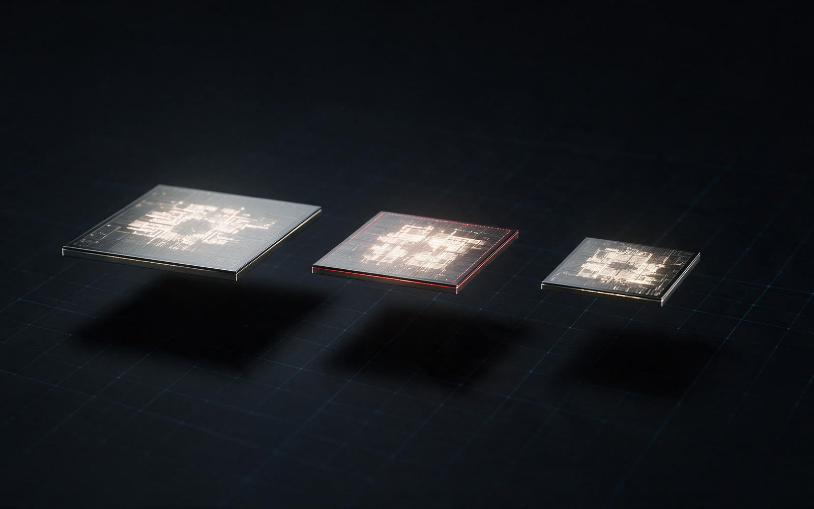
Sensory intake runs on ultra-low-power 55 nm ISPs. High-compute subsystem processing takes 12 nm. And the balanced 28 nm node carries core control — and the next-generation LLM IC. Strategic allocation, not one-size-fits-all.
02
Vertically integrated, cross-domain
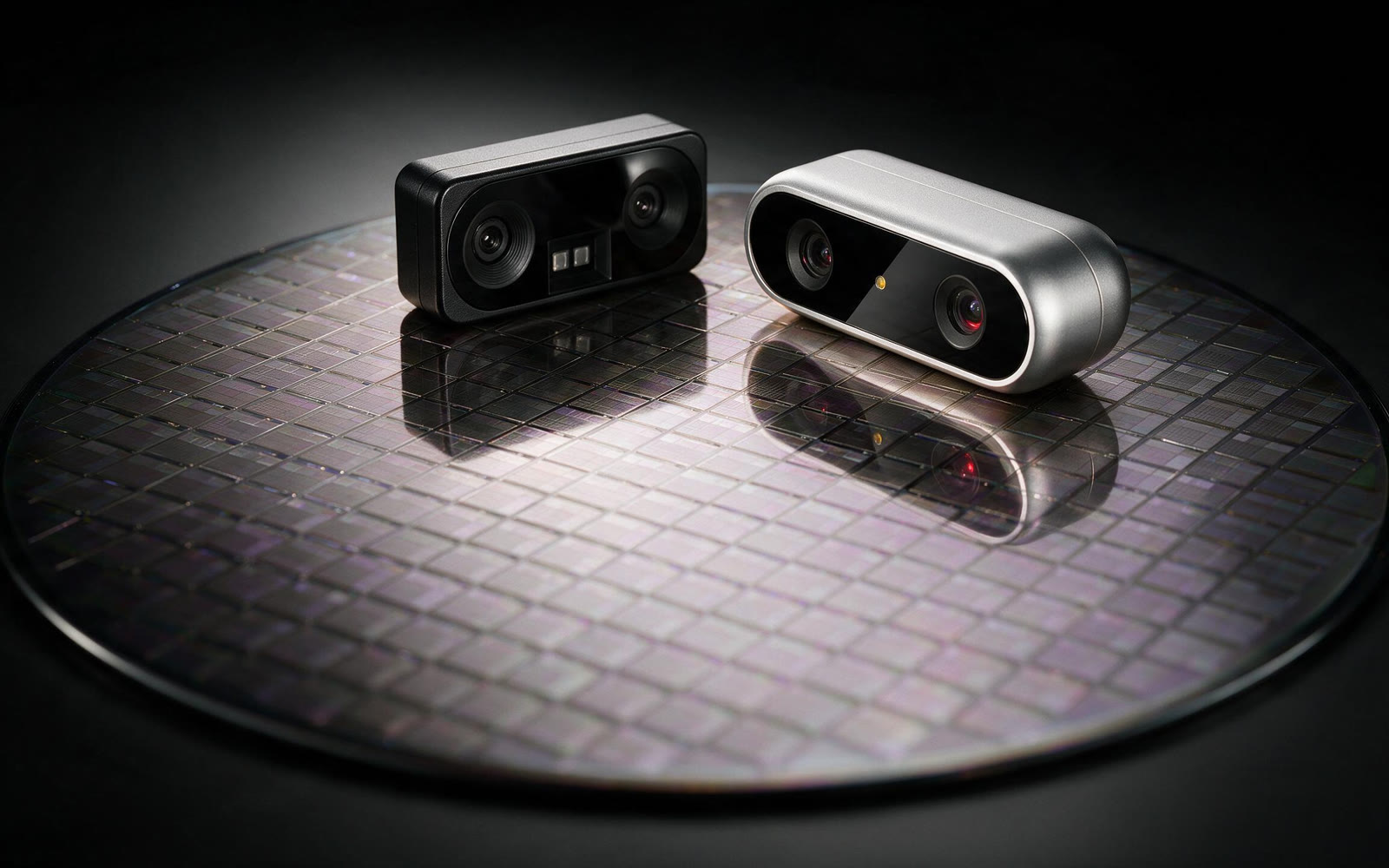
Silicon, active stereo sensors, dot-projector optics, and customized sub-systems ship from one roadmap — vertically integrated hardware that serves different volumes and domains, from consumer robotics to industrial AMRs. One of the only Taiwanese design houses with multiple MP-ed ICs and system-level deployments.
Strategic node allocation
| TSMC 12 nm | Subsystem processing — high-compute efficiency for complex, localized robotic actions |
|---|---|
| TSMC 28 nm | Core control & next-gen LLM IC — balanced power-to-performance for edge AI tape-outs |
| TSMC 55 nm | ISP — ultra-low-power, dedicated continuous sensory intake |
Start with a dev kit, scale to a fleet.
Get XINK SENSE on your bench this week, or talk to us about the full stack.